Hypervisor rootkit detection strategies

Keith Adams of VMware has a blog where he writes about his experiences virtualizing x86. In a well-written post, he discusses resource utilization techniques for detecting a hypervisor rootkit, including the TLB method described in his recent HotOS paper (alternate link).

We better find a way to derail Keith before he brainstorms any more of our techniques, although we have a reasonable claim that a co-author has published on TLB usage first. :-) Good thing side channels in an environment as complex as the x86 hardware interface are limitless!

Undetectable hypervisor rootkit challenge

I’m starting to get some queries about the challenge Tom, Peter, and I issued to Joanna. In summary, we’ll be giving a talk at Blackhat showing how hypervisor-based rootkits are not invisible and the detector always has the fundamental advantage. Joanna’s work is very nice, but her claim that hypervisor rootkits are “100% undetectable” is simply not true. We want to prove that with code, not just words.

Joanna recently responded. In summary, she agrees to the challenge with the following caveats:

  • We can’t intentionally crash or halt the machine while scanning
  • We can’t consume more than 90% of the CPU for more than a second
  • We need to supply five new laptops, not two
  • We both provide source code to escrow before the challenge and it is released afterwards
  • We pay her $416,000

The first two requirements are easy to agree to. Of course, the rootkit also shouldn’t do either of those or it is trivially detectable by the user.

Five laptops? Sure, ok. The concern is that even a random guess could be right with 50% probability. She is right that we can make guessing a bad strategy by adding more laptops. But we can also do the same by just repeating the test several times. Each time we repeat the challenge, the probability that we’re just getting lucky goes down significantly. After five runs, the chance that we guessed correctly via random guesses is only 3%, the baseline she established for acceptability. But if she wants five laptops instead, that’s fine too.

I don’t have a problem open-sourcing the code afterwards. However, I don’t see why it’s necessary either. We can detect her software without knowing exactly how it’s implemented. That’s the point.

The final requirement is not surprising. She claims she has put four person-months work into the current Blue Pill and it would require twelve more person-months for her to be confident she could win the challenge. Additionally, she has all the experience of developing Blue Pill for the entire previous year.

We’ve put about one person-month into our detector software and have not been paid a cent to work on it. However, we’re confident even this minimal detector can succeed, hence the challenge. Our Blackhat talk will describe the fundamental principles that give the detector the advantage.

If Joanna’s time estimate is correct, it’s about 16 times harder to build a hypervisor rootkit than to detect it. I’d say that supports our findings.

[Edit: corrected the cost calculation from $384,000]

Taxonomy of glitch and side channel attacks

There are a number of things to try when developing such attacks, depending on the device and countermeasures present. We’ll assume that the attacker has possession of several instances of the device and a moderate budget. This limits an attacker to non-invasive and slightly invasive methods.

Timing attacks work at the granularity of entire device operations (request through result) and don’t require any hardware tools. However, hardware may be used to acquire timing information, for example, by using an oscilloscope and counting the clock cycles an operation takes. I call this observation point external since only information about the entire operation (not its intermediate steps) is available. All software, including commonly used applications or operating systems, need to be aware of timing attacks when working with secrets. The first published timing attack was against RSA, but any kind of CPU access to secret data can reveal information about that data (e.g., cache misses.)

A common misconception is that noise alone can prevent timing attacks. Boneh et al disproved this handily when they mounted timing attacks against OpenSSL over a WAN. If there is noise, just take more measurements. Since noise is random but the key is constant, noise tends to average out the greater your sample size.

Power, EM, thermal, and audio side channel attacks measure more detailed internal behavior throughout an operation. If the intermediate state of an operation is visible in a timing attack, I classify it as an internal side channel attack as well (e.g., Percival’s cache timing attack.) The granularity of measurement is important. Thus, thermal and audio attacks are less powerful given the slow response of the signal compared to the speed of the computation. In other words, they have built-in averaging.

Simple side channel attacks (i.e. SPA) involve observing differences of behavior within a single sample. The difference in height of the peaks of power consumption during a DES operation might indicate the number of 1 bits in the key for that particular round. Since most crypto is based on an iterative model, similarities and differences between each iteration directly reflect the secret data being processed.

Differential side channel attacks (i.e. DPA) are quite a bit different. Instead of requiring an observable, repeatable difference in behavior, any slight variation in behavior can be leveraged using statistics and knowledge of cipher structure. It would take an entire series of articles to explain the various forms of DPA, but I’ll summarize by saying that DPA can automatically extract keys from traces that individually appear completely random.

Glitch attacks (aka fault induction) involve deliberately inducing an error in hardware behavior. They are usually non-invasive but occasionally partially invasive. If power lines are accessible, the power supply can be subjected to a momentary excessive voltage or a brown-out. Removing decoupling capacitors can magnify this effect. If IO lines are accessible, they can be subjected to high-frequency analog signals in an attempt to corrupt the logic behind the IO buffer. But usually these approaches can be prevented by careful engineering.

Most glitch attacks use the clock line since it is especially critical to chip operation. In addition to over-voltage, complex high-frequency waveforms can induce interesting behavior. Flip-flops and latches have a timing parameter called “setup and hold” which indicates how long a 0 or 1 bit needs to be applied before the hardware can remember the bit. High frequency waveforms at the edge of this limit cause some flip-flops to register a new value (possibly random) and others to keep their old value. Natural manufacturing variances mean this is impossible to prevent. Pulse, triangle, and sawtooth waveforms provide more possibilities for variation.

Optical and EM glitch attacks induce faults using radiation. Optical attacks are partially invasive in that the chip has to be partially removed from its package (decapping). EM attacks can usually penetrate the housing. The nice thing about this glitching approach is that individual areas of the chip can be targeted, like RAM which is particularly vulnerable to bit flips. Optical attacks can be done using a flash bulb or laser pointer.

With more resources, tools like FIB workstations become available. These allow for fully invasive attacks, where the silicon is modified or tapped at various places to extract information or induce insecure behavior. Such tools are available (Ross Anderson’s group has been using one since the mid 90’s) but are generally not used by the hobbyist hacker community.

Hardware design and glitch attacks

The first step in understanding glitch attacks is to look at how hardware actually works. Each chip is made up of transistors that are combined to produce gates and then high-level features like RAM, logic, lookup tables, state machines, etc. In turn, those features are combined to produce a CPU, video decoder, coprocessor, etc. We’re most interested in secure CPUs and the computations they perform.

Each of the feature blocks on a chip are coordinated by a global clock signal. Each time it “ticks”, signals propagate from one step to another and among the various blocks. The speed of propagation is based on the chip’s architecture and physical silicon process, which together determine how quickly the main clock can run. This is why every CPU has a maximum (but not minimum) megahertz rating.

In hardware design, the logic blocks are made up of multiple stages, very much like CPU pipelining. Each clock cycle, data is read from an internal register, passes through some combinational logic, and is stored in a register to wait for the next clock cycle. The register can be the same one (i.e. for repeated processing as in multiple rounds of a block cipher) or a different one.

chippipe1.png

The maximum clock rate for the chip is constrained by the slowest block. If it takes one block 10 ns to propagate a signal from register to register, your maximum clock rate is 100 MHz, even if most of the other blocks are faster. If this is the case, the designer can either slice that function up into smaller blocks (but increase the total latency) or try to redesign it to take less time.

A CPU is made up of multiple blocks. There is logic like the ALU or branch prediction, RAM for named registers and cache, and state machines for coordinating the whole show. If you examine an assembly instruction datasheet, you’ll find that each instruction takes one or more clocks and sometimes a variable number. For example, branch instructions often take more clock cycles if the branch is taken or if there is a branch predictor and it got it wrong. As signals propagate between each block, the CPU is in an intermediate state. At a higher level, it is also in an intermediate state during execution of multi-cycle instructions.

As you can see from all this, a CPU is very sensitive to all the signals that pass through it and their timing. These signals can be influenced by the voltage at external pins, especially the clock signal since it is distributed to every block on a chip. When signals that have out-of-spec timing or voltage are applied to the pins, computation can be corrupted in surprisingly useful ways.

Glitch attacks revealed

(First in a series of articles on attacking hardware and software by inducing faults)

One of the common assumptions software authors make is that the underlying hardware works reliably. Very few operating systems add their own parity bits or CRC to memory accesses. Even fewer applications check the results of a computation. Yet when it comes to cryptography and software protection, the attacker controls the platform in some manner and thus faulty operation has to be considered.

Fault induction is often used to test hardware during production or simulation runs. It was probably first observed when mildly radioactive material that is a natural part of chip packaging led to random memory bit flips.

When informed that an attacker in possession of a device can induce faults, most engineers respond that nothing useful could come of that. This is a similar response to when buffer overflows were first discovered in software (“so what, the software crashes?”) I often find this “engineering mentality” gets in the way of improving security, even insisting you must prove exploitability before fixing a problem.

A good overview paper is “The Sorcerer’s Apprentice Guide to Fault Attacks” by Bar-el et al. In their 1997 paper “Low Cost Attacks on Tamper Resistant Devices,” Anderson and Kuhn conclude:

“We have improved on Differential Fault Analysis. Rather than needing about 200 faulty ciphertexts to recover a DES key, we need between one and ten. We can factor RSA moduli with a single faulty ciphertext. We can also reverse engineer completely unknown algorithms; this appears to be faster than Biham and Shamir’s approach in the case of DES, and is particularly easy with algorithms that have a compact software implementation such as RC5.”

This is quite a powerful class of attacks, and is sometimes applicable to software-only systems as well. For instance, a signal handler often can be triggered from remote, inducing faults in execution if the programmer wasn’t careful.

Of course, glitch attacks are most applicable to smart cards, HSMs, and other tamper-resistant hardware. Given the movement to DRM and trusted computing, we can expect to see this category of attack and its defenses become more sophisticated.  Why rob banks? Because that’s where the money is.

Anti-debugging techniques of the past

During the C64 and Apple II years, a number of interesting protection schemes were developed that still have parallels in today’s systems. The C64/1541 disk drive schemes relied on cleverly exploiting hardware behavior since there was no security processor onboard to use as a root of trust. Nowadays, games or DRM systems for the PC still have the same limitation, while modern video game systems rely more on custom hardware capabilities.

Most targeted anti-debugger techniques rely on exploiting shared resources. For example, a single interrupt vector cannot be used by both the application and the debugger at the same time. Reusing that resource as part of the protection scheme and for normal application operations forces the attacker to modify some other shared resource (perhaps by hooking the function prologue) instead.

One interesting anti-debugger technique was to load the computer’s protection code into screen memory. This range of RAM, as with modern integrated video chipsets, is regular system memory that is also mapped to the display chip. Writing values to this region changes the display. Reading it returns the pixel data that is onscreen. Since it’s just RAM, the CPU can execute out of it as well but the user would see garbage on the screen. The protection code would change the foreground and background colors to be the same, making the data invisible while the code executed.

When an attacker broke into program execution with a machine language monitor (i.e., debugger), the command prompt displayed by the monitor would overwrite the protection code. If it was later resumed, the program would just crash because the critical protection code was no longer present in RAM. The video memory was a shared resource used by both the protection and the debugger.

Another technique was to load code into an area of RAM that was cleared during system reset. If an attacker reset the machine without powering it off, the data would ordinarily still be present in RAM. However, if it was within a region that was zeroed by the reset code in ROM, nothing would remain for the attacker to examine.

As protection schemes became stronger in the late 1980’s, users resorted to hardware-based attacks when software-only copying was no longer possible. Many protection schemes took advantage of the limited RAM in the 1541 drive (2 KB) by using custom bit encoding on the media and booting a custom loader/protection routine into the drive RAM to read it. The loader would lock out all access by the C64 to drive memory so it could not easily be dumped and analyzed.

The copy system authors responded in a number of ways. One of them was to provide a RAM expansion board (8 KB) that allowed the custom bit encoding to be read all in one chunk, circumventing the boundary problems that occurred when copying in 2 KB chunks and trying to stitch them back together. It also allowed the protection code in the drive to be copied up to higher memory, saving it from being zeroed when the drive was reset. This way the drive would once again allow memory access by the C64 and the loader could be dumped and analyzed.

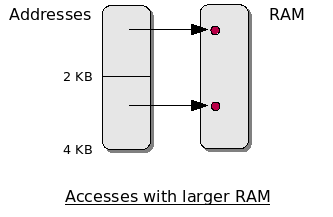
Protection authors responded by crashing the drive when expanded RAM was present. With most hardware memory access, there’s a concept known as “mirroring.” If the address space is bigger than the physical RAM present, accesses to higher addresses wrap around within the actual memory. For example, accesses to address 0, 2 KB and 4 KB would map to the same RAM address (0) on a 1541 with stock memory. But on a drive with 8 KB expanded RAM, these would map to three different locations.

1541ram1.png

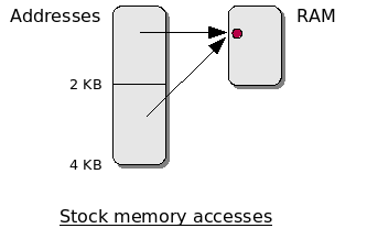
One technique was to scramble the latter part of the loader. The first part would descramble the remainder but use addresses above 2 KB to do its work. On a stock 1541, the memory accesses would wrap around, descrambling the proper locations in the loader. On a modified drive, they would just write garbage to upper memory and the loader would crash once it got to the still-scrambled code in the lower 2 KB.

1541ram2.png

These schemes were later circumvented by adding a switch to the RAM expansion that allowed it to be switched off when it wasn’t in use, but this did add to the annoyance factor of regularly using a modified drive.